Antennas Into PCBs
Antennas are crucial for wireless connectivity in PCBs. But they come with their own set of challenges that require specialized knowledge and techniques to overcome. This article explores the key principles and best practices to unlock the full potential of integrated antenna solutions.
PCB antennas must fit in a limited physical area. This may limit their performance in terms of radiation pattern and efficiency. Furthermore, PCBs have many other traces and components that can cause interference with the antenna. These can include high speed digital circuits, memories, and IO buses. Careful PCB layout and grounding can help mitigate these issues.
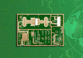
The RF front end of the antenna must also be properly matched to the rest of the rf circuit board. This is important to minimize characteristic impedance and impeded losses. This can be accomplished by placing the matching network close to the antenna and using a transmission line with a straight path between the feeding lines and the radiating elements (see Fig. 2). A careful analysis of the antenna’s performance in a particular environment is also critical to ensure that it operates as intended.
RF and microwave signals are very sensitive to noise, especially when they’re operating at higher frequencies. This can introduce ringing, reflection, and other undesirable effects into the circuit. PCB design techniques can be used to minimize these problems, including ensuring that the antenna is free of nearby components and traces, and that it’s shielded from the case.
Integrating Antennas Into PCBs
Antennas can also be impacted by EMI and EMC considerations, such as crosstalk between adjacent radiating antennas or with other electronic devices in the same physical space. This can be caused by metals like the case of the device or other conductive elements on the PCB. Taking measures to mitigate these effects can be challenging but not impossible, and it’s often a case of balancing the desired performance with the available space on the device.
One way to reduce the complexity of integrating an antenna into an RF circuit board is to use a system-in-package (SiP) microcontroller and radio frequency front end combination. This approach reduces the amount of RF circuitry required and can dramatically cut the development costs associated with building an IoT product by eliminating the need to build a separate MCU and antenna. However, this still leaves the antenna integration challenge for engineers to address. An alternative is to pair the SiP with either a PCB trace antenna or an integrated chip antenna.
Both options offer the advantages of space efficiency, but the latter requires a more complex manufacturing process to accommodate the MCU and antenna and can increase time to market. Getting the right advice at the start of your project can help you choose the most effective solution for your needs. An experienced RF engineer can provide invaluable insights into everything from antenna placement to ground plane size. By leveraging these insights, you can create an RF circuit board that provides robust wireless connectivity in the smallest possible devices.